The rapid growth of semiconductor materials for nanoscale applications has driven the development of high-quality crystalline thin films crucial for advanced technologies. Key methods like chemical vapor-phase deposition (CVD) and its variations—MOVPE, PECVD, and MBE—are now essential in the electronics industry. Over the past thirty years, advancements in these techniques have facilitated the production of epi-wafers for various semiconductor applications, including CMOS, HEMT, RF, power, and laser technologies.
The Computer Aided Design (CAD) software can help to realize the deep insight with atomistic scale solution and the proper understanding of the microscopic issues and challenges associated with these reactors based epitaxial growth processes.
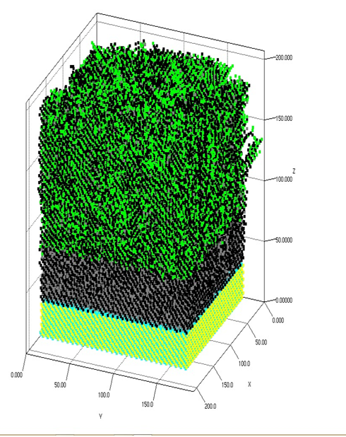
The TNL-EpiGrow simulator provide real-time reactor growth conditions through simulation for accurate trial experiments, reducing labor, conserving gases, lowering processing costs, and identifying defects.
The TNL-EpiGrow simulator supports multiple epitaxy processes for analyzing vapor phase epitaxy methods like CVD, PECVD, MOCVD, and MBE. It aids in optimizing growth processes for semiconductors, insulators, metals, superconductors, and magnetic materials.
TNL-Optimizer enables design of experiments (DOE) to fine-tune input parameters for producing high-quality crystalline films with minimal defects, enhancing the epitaxial growth of semiconductors, oxides, insulators, metals, and superconductors.
Epitaxial Growth processes inbuilt in the TNL-EpiGrow simulator are:
Graphical User Interface (GUI)
Windows based Application
Various Semiconductor Materials Database
Thermal chemical kinetics
Plasma enhaced chemical kinetics
Users' defined input growth conditions
To handle various gas phase kinetics
To handle various surface phase kinetics
Import users' specific gas & surface phase kinetics
Inbuilt precursor & carrier gases database
kMC based Adsorption, hopping & desorption rates
Reactor geometry parameters as input
molecular beams with various Knudsen cells
Impact of Schwoebel-Enrich barrier energy
Impact of incorporation barrier energy
Impact nearest neighbor energy
Mapping each & every atom in each monolayer
Point Defects density with location on lattice
Line Defects density in lattice
Stacking Fault density in lattice
Surface profiles i.e. Roughness
Strain measurement
Lattice Parameter
Optimization of input parameters
Optimization of chemical kinetics
Reduction in waste during experimentation
Ability to deal with different reactive species and reactor geometries
On-line process control