The semiconductor device industry requires defects free and high quality thin films for development of high performance devices. Various techniques e.g. XRD, AFM, FTIR, SEM, TEM, XPS, Ellipsometry etc. are used to identifying crystallinity and preferred crystal orientation, defects etc.
From theoretical point of view, people use Ab-initio methods e.g.Hartree-Fock or Density Functional Theory (DFT) based approaches by utilizing a variational approach to calculate the ground state energy of a many-body system Computationally very expensive, sometimes require massively parallel computers
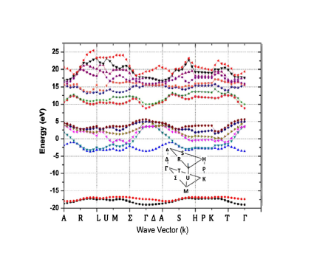
TNL material characterization tools are computationally less expensive a relatively easy for generating electronic and optical properties of semiconductor materials with accuracy. Each and every electron contribution during character Carrier dynamics through solution of Boltzmann transportation equation (BTE) with inclusion of various non-linear scattering mechanisms over few valleys or full band structure under influence of external forces provide accurute and relaible output. The output results are use to calibrate the experimental findings. Graphical User Interface (GUI) feature of each simulator makes it user friendly, easy to learn and run.


