The Tech Next Lab (TNL) offer modeling & PDK based design services with fabrication facilities from specific foundry based on customer needs. The core of competancy includes design, development and fab services for tecnological domains as below:
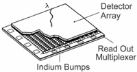
Infrared Photodetectors
Expertise for HgCdTe (MCT), InGaAs, InSb based SWIR, MWIR & LWIR detector modeling with Foundry Support.
LED, Solar Cell, LASER, Image Sensors, Charge Coupled devices etc.
Optical Devices
Radiation Detectors
Si based TID & LET detectors, CdTe, CdZnTe based radiation detectors with Foundry Support.
 >
>
CMOS Applications
Modeling Services of Si CMOS including FinFET, FDSOI, GAA, Nanosheets etc..
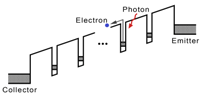
Quantum Well device
Modeling and simulation services of Quantum well, Quantum Wire, Quantum Dot & Superlattice structures with Foundry Support.
Power Devices
We supports epitaxial growth, material characterization & device application with TNL TCAD tools especially for wideband gap based technologies e.g. GaN, SiC, Ga2O3.