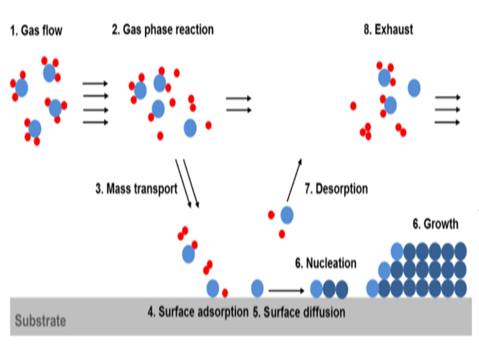


Atomistic Epitaxial Growth Processes
The explosive growth of the semiconductor materials, the industry has caused a rapid evolution of thin-film materials that lend themselves to the fabrication of state-of-the-art semiconductor devices. The research technique named chemical vapor-phase deposition (CVD) along with its variants e.g. Metalorganic vapor-phase epitaxy (MOVPE), also known as organometallic vapor-phase epitaxy (OMVPE) or metalorganic chemical vapor deposition (MOCVD), plasma enhanced chemical vapor deposition (PECVD) and molecular beam epitaxy (MBE) etc have shown several unique advantages. These growth techniques have developed into the most widely used techniques for thin film preparation in electronics technology. In the last three decades, tremendous advances have been made in the science and technology of thin films prepared by means of MBE, CVD, PECVD, MOCVD reactors etc for production of epi-wafer for CMOS, RF, power, laser and other semiconductor industries, upon reactor’s geometries and specific technology applications.
The Computer Aided Design (CAD) software can help to realize the deep insight with atomistic scale solution and the proper understanding of the microscopic isues and challenges associated with these reactors based epitaxial growth processes.
To reduce the development cost, time and manpower consumption & to cater semiconductor material industry needs, TNL Epitaxial Material Growth Computer-Aided Design tools will be useful and provide flexibilities to run design of experiments (DOE) to achieve optimum conditions and high quality film with real reactor’s geometries and various other input conditions.
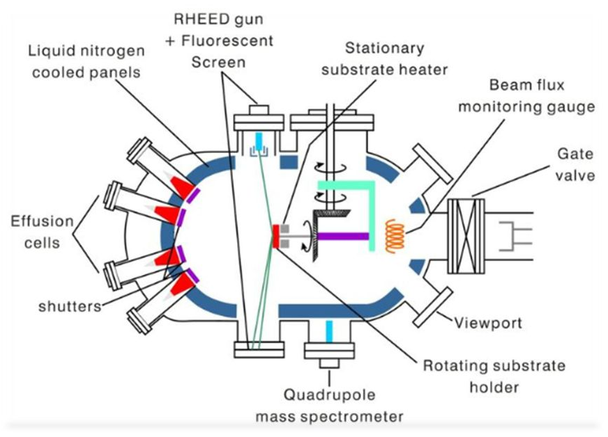
MBE Simulator
UHV Chamber ConditionsUltra High Purity Materials
Elemental & compound semiconductors material database
Multiple Effusion Cells
Flux controlled by Temperature
Distinction between types of Defects