TNL TCAD
(Atomistic TCAD for Epitaxy, Material & Device Modeling)
Menu
Downloads
Contact Us
Products
Family of TCAD Software/a>
Epitaxy Solutions
Deposition Reactors
TNL-MBE Simulator
TNL-CVD Simulator
TNL-MOCVD (Showerhead) Simulator
TNL-MOCVD (Injector) Simulator
TNL-PECVD Simulator
Material Characterization
Material Characterization
TNL-FB Simulator (Full Band)
TNL-EM Simulator (Carrier Mobility)
TNL-TS Simulator (HOT Carrier Dynamics)
Device Characterization
Device Characterization
TNL-PD Simulator (Particle based device 2D)
TNL-PD Simulator (Particle based device 3D)
Visualization Tools
Structure & Graphs
TNL-StrView (3D Structure Visualization)
TNLPlot (Graphical Analysis)
Services
Modeling & Foundry Support
Epitaxial Growth Modeling
Material Characterization Modeling
Device Modeling & Foundry Support
Latest News & Updates
Latest News & Updates
News
Events
Publications
Company Profile
Company Profile
About us
Career
Technology Transfers
Success Stories
Indian Defence (DRDO)
Indian Space (ISRO)
News and Latest Updates
Home
>> Publications
Latest News & Updates
News
Events
Publications
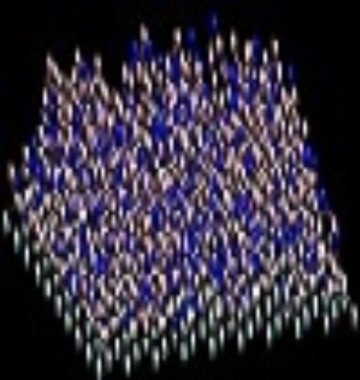
Atomistic simulation solution of MBE epitaxy of 6.1-Å semiconductors multiple QW heterostructures
Uncovering the influence of nitridation on the dislocation density at atomistic scale in III-Nitrides MOCVD/MOVPE epitaxy process
MOCVD/MOVPE epitaxy of group III-V nitride with atomistic Prospective & cost Effectiveness
Full Electronic Band Structure Characterization of Al‑Doped ZnO Nanocrystalline Films Through Simulation.
Epitaxy Solution of the III-V Antimonides/Arsenides Quantum Well Heterostructure for IR Detector Applications: TNL-EpiGrow Simulator.
MOCVD Epitaxy Solution of HgCdTe Heterostructures for Infrared Detectors through An Innovative Simulation Technique.
MBE Epitaxy Solution of the Quantum Well Heterostructure: Atomistic TNL-EpiGrow Simulator.
Defect Analysis of MBE Reactor Grown HgCdTe on Si, GaAs, GaSb, CZT Substrates Through TNL-EPIGROW Simulator.
MOCVD/MOVPE Epitaxy Solution of Group III-V Nitride with Atomistic Prospective and Cost Effectiveness
Epitaxy of III-V Nitrides with Strain Relief Layers Analysis— TNL EpiGrow Simulator.
An Atomistic insights for Predictive In-Silico Chemical Vapor Deposition.
Dislocations/Defects analysis in III-V nitrides - a cost effective MOCVD epitaxy solution.
Defect analysis of HgCdTe deposited on GaAs, GaSb, CZT through MBE process: TNL-EpiGrow Simulator.
Impact of various defects on Carrier Field Mobility in ZnO thin films.
Full Electronic Band structure characterization of ZnO Nanorod
Nonlinear Ultrafast carrier’s dynamics with scattering rate saturation in Ge thinfilms.
An Innovative Model for Electronic Band Structure Analysis of Doped and Un-Doped ZnO.
An innovative technique for electronic transport model of group-III nitrides.
Numerical simulation of InxGa1-xAs/InP PIN photodetector for optimum performance at 298 K.
HEMT growth to Device: Advances in Electrical Control and Signal Systems, Chapter 61, ISBN No. -9789811552618, 2020.
"Full Electronic Band Structure Analysis of Cd Doped ZnO Thin Films Deposited by SOL-GEL SPIN COATING METHOD ".
"An innovative approach for controlled epitaxial growth of GaAs in real MOCVD reactor environment".
"Infrared Phototectors: Some techniques for Modeling & Simulation, 2018.
Numerical Study of Dual band (MW/LW) IR Detector for Performance Improvement, Defense Science journal, Vol 67, No 2, pp. 141-148, 2017.
EpiGrow Simulator Technical details.
Semiconductor Materials Mobility Characterization Tutorial
ors through An Innovative Simulation Technique